Electrical and Computer Engineering
Ferromagnetic Semiconductor and Spintronic Devices
Spring 2025, Volume 23, Issue 2
Zijian Shang ’25, Roman Sobolewski*
DOI: 10.47761/APLC2947
Abstract
Ferromagnetic semiconductors have been widely used and studied for their functionalities in spin manipulation through semiconductor-compatible processes. Novel phenomena such as giant magnetoresistance (GMR) and tunneling magnetoresistance (TMR) effects contribute to the development and applications of spintronic devices.
Introduction
The trend of the microelectronic industry is predicted by Moore’s law, a concept proposed by Intel co-founder Golden Moore in 1965. Moore’s law states that the number of transistors per die will double every two years, which has been true for nearly half a century. Today, it is widely acknowledged that Moore’s law has approached its limit. While the discipline of traditional charge-based electronics is facing an inevitable end of innovation, spintronics, an emerging field, offers an alternative by using both an electron’s electric charge and spin angular momentum to exploit novel functions, showing great promise for high speed, power efficient logic, and electronic devices with nonvolatile memory [1].
Conventional electronic devices use the two electrons’ intrinsic properties, charges and spins, separately. For instance, devices related to manipulation of charge current are transistors, diodes, etc; while magnetic materials use spin to make devices such as magnetic hard drives and sensors. The ferromagnetic semiconductor, a semiconductor material with ferromagnetic properties, has the potential to create devices due to its unique combination of magnetic order and semiconducting properties. After the utilization of molecular beam epitaxy in the 1980s, III-V-based ferromagnetic semiconductors (FMSs), in particular (Ga,Mn)As, became the subject of extensive research [2].
Basics of Spintronic Devices
The spin-based electronics is a technique that combines traditional electric charge properties and spin-based functionality. Understanding the spin carriers’ transport mechanisms, such as spin injection and spin relaxation is crucial for the development of spintronic devices.
Spin Injection
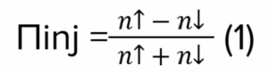
One of the ferromagnetic properties is the unequal number of spin-up and spin-down electrons at the Fermi-level. Therefore, it is often chosen to be a spin injector. In this case, assuming that a majority of electrons spin up, the spin-up electrons’ density of states is higher than the spin-down electrons’ density of states, which results in unequal conductivity for spin-up and spin-down electrons [3]. Therefore, when charge current passes through ferromagnetic material Icharge = I↑+I↓, spin-up electrons, as the majority, have higher conductivity, resulting in spin current Ispin = I↑ − I↓. When the spin current crosses the ferromagnet/antiferromagnet interface, the conductivities for both spin states become equal, resulting in spin accumulation at the interface [4]. Spin polarization is used to describe the efficiency of injection, which is defined as [1].
The conductivity of the ferromagnet is much larger than that of the non-ferromagnetic material, which induces a mismatch issue that can cause reflection of the spin carrier at the ferromagnet/antiferromagnet interface [1]. To solve this, the installation of a tunneling barrier is proposed by placing a high-resistance tunnel barrier between the ferromagnet and the antiferromagnet. The tunnel barrier allows the quantum tunneling of electrons to dominate the transport mechanism, which reduces the probability of reflection. The probability of quantum tunneling is proportional to the carriers’ density of states. The majority spin carrier has a larger density of states, and therefore it is more likely to tunnel through the barrier, which increases the spin polarization [1].
Giant Magnetoresistance
Giant Magnetoresistance is observed from heterostructure where two ferromagnetic materials are separated by an insulator which refer to magnetic tunneling junction (MTJ). It refers to the phenomenon that the electrical resistance strongly depends on the relative orientations of magnetization in adjacent magnetic layers in heterostructure such as ferromagnet(FM) — nonmetal(NM) — FM (for instance, parallel or antiparallel configurations). The parallel and antiparallel geometries are explained in Figure 1. The magnetization direction can be controlled, for example, by applying an external magnetic field [5].
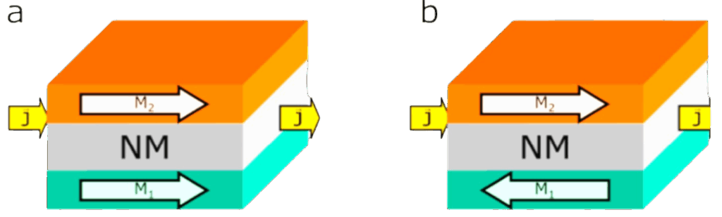
Figure 1. Left: parallel configuration, right: antiparallel configuration [5].
Tunnel Magnetoresistance
Tunnel magnetoresistance (TMR) is observed from MTJ. It refers to the change of electrical resistance with the change of ferromagnetic layers’ antiparallel and parallel orientation.
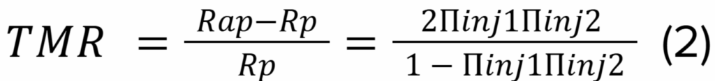
Rap is the electrical resistance of the antiparallel state and Rp is the electrical resistance of the parallel state. A high TMR means the device can effectively distinguish parallel and antiparallel states of the heterostructure which is useful in storing binary information. Πinj1 and Πinj2 are spin polarizations for the first FM and second FM respectively [6]. This effect makes MTJ a core component of nonvolatile memory devices. MTJ is considered a core component of the nonvolatile memory device.
Spin Relaxation
Like attenuation of electromagnetic waves, spin “attenuates” in non-ferromagnetic material due to four mechanisms. The Elliott–Yafet mechanism states the electrons flip their spin orientation scattered off impurities or phonons with tiny probability which can equilibrate the number of spin-up and spin-down electrons [1]. The D’yakonov Perel mechanism states that the scattering events cause random electron momentum, thus the electrons change their spin orientation randomly when they process the effective magnetic field resulting from spin-orbital coupling with atoms [1][7]. The Bir–Aronov–Pikus mechanism states the change of electrons’ spin due to their spin exchange with holes in the p-type semiconductor which accelerates the EY mechanism in the valence band and holes are more easily affected by spin-orbital coupling [1]. The hyperfine coupling states the change of spin orientation from an interaction between electrons’ magnetic moment and the nucleus magnetic moment [1]. The specific material (e.g., semiconductor type, doping, flaws, strain) and the operating conditions (e.g., temperature, magnetic field, electric field, confinement) determine the relative strength of each mechanism.
Ferromagnetic Semiconductor: (Ga,Mn)As
Ferromagnetism in (Ga,Mn)As
The ferromagnetic behavior within a semiconductor is induced by doping the material with magnetic impurities, typically transition metals such as manganese (Mn). In FMSs, the alignment of magnetic moments in the same direction leads to a significant growth in magnetic susceptibility, which allows FMs to become strongly magnetized in weak external magnetic fields [8]. The coupling of magnetic and electronic properties in FMSs makes it an ideal material for spintronic devices which offers efficiency in spin generation, transportation, and detection.
After the utilization of MBE in 1980s [2], a significant advancement of ferromagnetic semiconductors was achieved by introducing III-V based dilute magnetic semiconductors (Ga,Mn)As which are created by alloying III-V semiconductors GaAs with magnetic ions Mn+2. The material was grown as a (Ga1−x,Mnx). As from 150°-300°C which contains x up to 20% and maintains a zinc-blende crystal structure [2]. In this material, Mn atoms replace Ga atoms in the crystal lattice which Mn acts as an acceptor in (Ga,Mn)As, making it a p-type semiconductor. When a hole introduced by Mn passes close to one magnetic moment introduced by Mn, it interacts with the magnetic field from the magnetic moment and aligns its spin to match. The hole then travels through the material and interacts with other Mn magnetic moments. This process constitutes an indirect exchange interaction between two Mn magnetic moments, resulting in all magnetic moments aligning in the same direction known as carrier-mediated ferromagnetism. This model is known as Ruderman-Kittel-Kasuya-Yosida (RKKY) which serves as the origin of ferromagnetism within (Ga,Mn)As [9]. This mechanism is demonstrated in Figure 2. Since the ferromagnetism resulted from the interaction between Mn spin and holes, increasing the concentration of Mn atoms introduces more magnetic spins and more holes, strengthening the coupling between spins which makes the magnetism tunable.
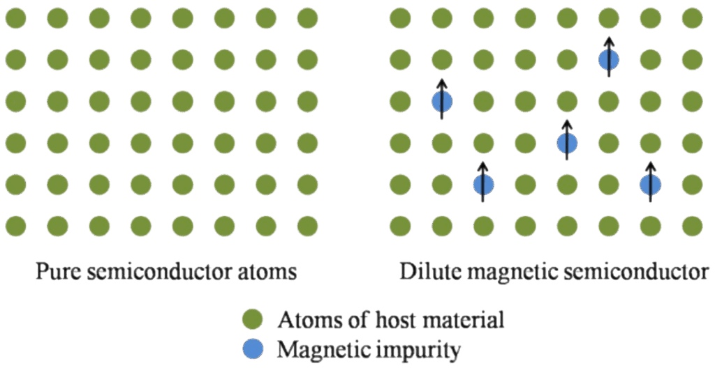
Figure 2. Doping Process of dilute magnetic semiconductor [10].
(Ga,Mn)As’s Application in Spintronic Devices
The use of (Ga,Mn)As as a spin injector reported by Y.Ohno in 1999 [11] and (Ga,Mn)As-based Magnetic tunneling junction has been reported by many researchers. One of the greatest advantages of (Ga,Mn)As is its compatibility with the existing GaAs technology which has been widely used in industry. Another advantage is its tunability, external means, such as light illumination and electrical gate voltage could be applied to (Ga,Mn)As [12], showing the possibility of tunable spintronic devices. In the article proposed by M. Overby [13], a thin layer of (Ga,Mn)As is coupled with a piezoelectric material (PZT). The strain field from the PZT aligns the magnetization of GaMnAs along one of its easy axes. Applying voltage to the PZT induces tensile or compressive strain in specific directions which tunes the magnetic anisotropy of (Ga,Mn)As, causing the magnetization to switch between two easy axes. The two stable magnetization orientations allow binary calculation for Magnetoresistive Random Access Memory (MRAM) devices. The magnetization state switch does not need a constant power supply which achieves nonvolatile memory storage and also low power consumption[13]. D. Chiba reported the capability of use (Ga,Mn)As to fabricate fully epitaxial MTJ structures in the entire single-crystalline form with high-quality interfaces with a large TMR ratio of 290% at 0.39 K [14].
Issues with (Ga,Mn)As
Curie temperature is an important criterion to evaluate ferromagnetic semiconductor. This is the threshold temperature at which a material can lose its ferromagnetic properties above this temperature. The highest curie temperature Tc is reported to be 200 K [15] which is still under room temperature. This limitation restricts the practical applications of (Ga,Mn)As to cryogenic environments. However, another ferromagnetic material (Ga, Mn)N is reported that it has a wide range of curie temperatures above room temperature along the change of Mn concentration[16]. This property marks (Ga, Mn)N as a promising candidate for room temperature spintronic application, even though (Ga, Mn)N is not as compatible as (Ga,Mn)As with existing technology.
Conclusion
By utilizing ferromagnetic semiconductor tunability of magnetic properties and magnetic tunneling junction, binary computation using electrons’ spin is made possible, paving the way for next-generation technologies. The integration of ferromagnetic semiconductors with existing semiconductor fabrication techniques also facilitates seamless compatibility with current technology, enabling hybrid systems that leverage both charge and spin. The potential for manipulation at room temperature broadens the application scope of spintronics from magnetoresistive random access memory to quantum computing, making ferromagnetic semiconductors pivotal in revolutionizing the future of information technology.
References
- D. H. B. D. B. Saha, “Spin-based semiconductor heterostructure de- vices,” in Comprehensive Semiconductor Science and Technology, vol. 6, pp. 563–614, 2011.
- M. Tanaka, “Recent progress in ferromagnetic semiconductors and spintronics devices,” Japanese Journal of Applied Physics, vol. 60, 2020.
- T. Taniyama, E. Wada, M. Itoh, and M. Yamaguchi, “Electrical and optical spin injection in ferromagnet/semiconductor heterostructures,” NPG Asia Materials, vol. 3, pp. 65–73, July 2011.
- M. R. Sears and W. M. Saslow, “Spin accumulation at ferromag- net/nonmagnetic material interfaces,” Phys. Rev. B, vol. 85, p. 014404, Jan 2012.
- I. Ennen, D. Kappe, T. Rempel, C. Glenske, and A. Hu¨tten, “Giant magnetoresistance: Basic concepts, microstructure, magnetic interactions and applications,” Sensors, vol. 16, no. 6, 2016.
- K. Y. Y. N. I.-L. P. B. D. P. P. B. H. A. Hirohata, “Review on spintronics: Principles and device applications,” Journal of Magnetism and Magnetic Materials, vol. 509, 2020.
- D. J. Griffiths, Introduction to Quantum Mechanics. Upper Saddle River, NJ: Prentice Hall, 1st ed., 1995.
- F. M. H. Ohno, “A ferromagnetic iii–v semiconductor: (ga,mn)as,” Solid State Communication, vol. 117, no. 3, pp. 179–186, 2000.
- I. A. Kokurin and N. S. Averkiev, “Model of localized state mediated exchange interaction and ferromagnetism in diluted magnetic semicon- ductors,” Phys. Rev. B, vol. 109, p. 214415, Jun 2024.
- S. Chahal, L. Phor, Suman, Ankita, A. Kumar, S. Duhan, and P. Kumar, “22 – role of defects and doping on magnetism in cerium oxide,” in Defect-Induced Magnetism in Oxide Semiconductors (P. Kumar, J. Pal Singh, and V. Kumar, eds.), Woodhead Publishing Series in Electronic and Optical Materials, pp. 529–546, Woodhead Publishing, 2023.
- Y. Ohno, D. K. Young, B. Beschoten, F. Matsukura, H. Ohno, and D. D. Awschalom, “Electrical spin injection in a ferromagnetic semiconductor heterostructure,” Nature, vol. 402, pp. 790–792, December 1999.
- J.-H. X. L. J. K. F. B. J. K. S. Lee, “Ferromagnetic semiconductor gamnas,” Material Today, vol. 12, pp. 14–21, 2009.
- A. C. L. P. R. X. L. J. K. F. M. Overby, “Gamnas-based hybrid multiferroic memory device,” arXiv, 2008.
- D. Chiba, F. Matsukura, and H. Ohno, “Tunneling magnetoresistance in (ga,mn)as-based heterostructures with a gaas barrier,” Physica E: Low-dimensional Systems and Nanostructures, vol. 21, no. 2, pp. 966– 969, 2004. Proceedings of the Eleventh International Conference on Modulated Semiconductor Structures.
- H. Wang, L. Chen, and J. Zhao, “Enhancement of the curie temperature of ferromagnetic semiconductor (ga,mn)as,” Science China Physics, Mechanics and Astronomy, vol. 56, no. 1, pp. 99–110, 2013.
- T. Hynninen, H. Raebiger, and J. von Boehm, “Structural and magnetic properties of (ga,mn)n from first principles,” Phys. Rev. B, vol. 75, p. 125208, Mar 2007.
About the Author
Zijian Shang is an undergraduate student majoring in Electrical and Computer Engineering at the University of Rochester. His research interests include spintronic devices, semiconductor heterostructure, and terahertz emissions.
Cite this Article
Shang, Z. and Sobolewski, R. (2025). Ferromagnetic Semiconductor and Spintronic Devices. University of Rochester, Journal of Undergraduate Research, 23(2). doi: 10.47761/APLC2947.
JUR | Creative Commons Attribution 4.0 BY International License